ngVLA Enabling Technologies
A key enabling technology for the ngVLA is a high-performance antenna design that is tailored to mass production. The ngVLA project and international and commercial partners produced a total of five competing conceptual designs for the antenna and subjected the development proposals to a competitive procurmenet process. Based on this assessment, the ngVLA project has recently partnered with mtex antenna technology gmbh on the design of the antenna.
Through an NSF Mid-Scale Innovations Program grant (MSIP, NSF award # 2034328), ngVLA is pursuing the preliminary design of the 18m main array antenna, inclusive of prototype construction and testing. This important award will allow the project to verify the performance of this critical system component and provide the assurance of performance and cost necessary to proceed to mass production in the construction phase of hte project.
The selected antenna design uses a novel cast and post-machined panel concept providing very high surface accuracy for observations up to 116 GHz, a bolted-node backup structure for ease of manufacture and assembly, and a wide diameter pedestal and azimuth bearing providing the requisite stiffness for pointing precision.
The resulting panel and backup structure concept lead to an octagonal main reflector shape. The 18m aperture is inscribed within this envelope (see figure to right) with the remaining area acting as a ground spillover shield to improve antenna noise temperature.
The preliminary design phase is expected to complete in late 2022, with prototype production and test activities scheduled for 2023 and 2024.
The Integrated Receiver Development (IRD) program is an ongoing effort to develop modern integrated receiver architectures for radio astronomy that digitize early and are easier to manufacture and maintain in large numbers compared to conventional assemblies. A wide range of novel technologies has been developed, patented, and licensed in order to make these advancements possible.
At the core of this program is the idea that modern integrated electronics and digital signal processing (DSP) are complementary to each other. Numerical signal processing is capable of providing a level of flexibility and precision that is unachievable using purely analog means, while integrated technology provides the stable calibrations and smooth spectral baselines that are needed for the DSP to realize its full potential.
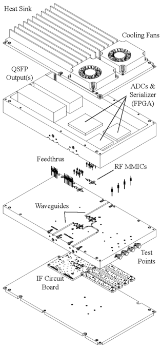
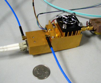
Each module is designed to immediately follow the cryogenic gain stage, and comprises everything that remains in the signal path operating at room temperature inside the antenna. This means that all conversions from RF-to-baseband, from analog-to-digital, and from copper-to-fiber are combined into a single, compact unit. Unique, multi-technology packaging and assembly techniques assure the best performance from micro-scale electronics with excellent digital-to-analog and channel-to-channel isolation.
The intrinsic receiver architecture is that of a single-stage, I/Q downconversion, using just one LO to get from the sky-frequency to baseband for immediate digitization. This allows for the earliest possible digitization in high-frequency systems while minimizing the potential for LO spurs and maximizing the instantaneous bandwidth for a given sample rate. Final separation of the I- and Q-channels into sidebands is deferred to the digital back-end for precise image-rejection, typically in excess of 50 dB, and is extremely stable over both time and temperature.
Integrated fiber-optic transceivers launch the raw, digital, I and Q data onto single-mode fibers with ranges of several meters to tens of kilometers. A unique, power-efficient, resolution-agnostic ADC-Serializer is under development which will further reduce power consumption. This will be supported in the back-end by a firmware IP block that can be installed on an FPGA platform and parses the data stream according to a novel, patent-protected algorithm. In this way, all the advantages of digital data transmission can be realized without most of the digital overhead normally required at the transmitter, such as bit-scrambling, packetizing, and framing.
While fabrication techniques vary by band, the overall concepts described above apply readily to the entire ngVLA frequency range. The most significant benefits of early digitization and the high level of stability afforded by these modules include reliability and scalability.
In collaboration with the National Research Council of Canada, the ngVLA project is investigating novel techniques for phasing the array. Fundamentally in a coherent array it is necessary to continuously align the wavefront from the source prior to correlation and beamforming. In the conventional approach, this is done using coherent LOs and digitizer clocks to do the high temporal-precision portion of this alignment, followed by digital delay and phase tracking according to a model of the wavefront delay for a known LO, and then periodic calibrator source observations to facilitate final alignment such that the “white light fringe”, on every correlated baseline, stays near zero relative delay. However, the first part of this process can be done differently by using free-running and incoherent clocks at each antenna, measuring the phase/frequency of each one in a common clock domain, and then digitally correcting the data—amounting to delay and phase corrections—prior to wavefront delay+phase correction and correlation and beamforming.
A block diagram of the general operation of the incoherent clocking method is shown in Figure 1. Optional down conversion and digitization of data at each antenna occurs using its own independent LO frequency aLOn(t). Digitized science data is sent to the correlator site along with a digital ‘tracer’ of aLOn(t) on a digital ‘tracer link’ (TL). The TL need only retain the real-time phase/frequency information of aLOn_tr(t) (the tracer frequency) inasmuch as needed to accurately extrapolate to the changing phase/frequency of aLOn_netLO(t) and aLOn_adc(t) that needs correcting in the data. The frequency of the digital tracer is measured and tracked to very high accuracy using a digital tone extractor, as indicated in Figure 2.
Of course, changes in the tracer link delay, τ_TL(t), for any appreciable TL length has an effect on the measured tracer phase/frequency vs time as indicated in Figure 1. To measure this, of course, a round-trip measurement is necessary: as shown in Figure 3, simply turn around the digital signal and measure its phase/frequency changes relative to the original digital tracer. Use these measurements to adjust the aLOn_tr(t) measurement to obtain a ϕTL_n_est(t)-corrected estimate, aLOn_tr_est(t), of the antenna LO and use it for correcting the data. Once aLOn_est(t) is available, it is used to re-sample and, if necessary, phase-correct the data in the “Re-sampler/corrector” circuit, shown in more detail in Figure 4. This circuit primarily consists of a real-time sample-by-sample interpolating O(80)-tap FIR filter, followed by a mixer to perform any phase corrections needed (for Nyquist zone-1 direct digitization, no phase corrections are required), driven by an aLOn_est- cLO phase synthesizer. What comes out is digital data corrected into the common cLO clock domain, ready for correlation (and beamforming).
A demonstration system will be developed by NRC starting in the fall of 2018.
Figure 1: Block diagram of the general operation of the incoherent clocking method. Courtesty of NRC.
Figure 2: Block diagram to measure and track the aLOn_tr tracer digital tone using a digital complex tone extractor. Courtesty of NRC.


